Péter Papp
Welcome to my personal page

Compact
switching power supply with digital control
for
Audio Amplifiers
A novel
two-stage high frequency power supply with high conversion
efficiency and galvanic insulation is proposed in the following
paper. Delivering the required high peak and long-term power for
a several thousands Watts range amplifier is not an easy job.
Conventional unregulated “50-60Hz toroidal transformer”
solutions suffers for heavy weight, bulky size and varying
output voltage behavior. Another problem is the bad power factor
with spike current draw due to its peak-rectification on the
secondary side of the transformer.
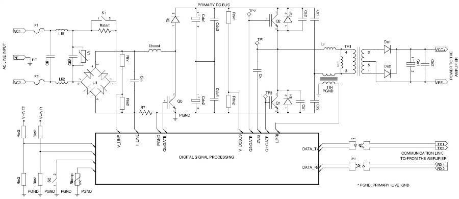
The proposed circuitry is shown on fig1. having two-stage topology. The input line
filter (Cfi1,2;Lfi1,2) is followed by a soft start circuitry and
and the rectifier bridge. The soft-start circuit (S1;Rstart)
eliminates the current bump of empty capacitors in the primary DC
bus when the power input is connected to the AC line. So the
charge current peak is limited around 30Apeak at the time of
power-up. A conventional Continous Current Mode (CCM) boost
converter regulated as an Active Power Factor Converter (APFC)
composed by Lboost;Qb and Db elements regulates the primary DC bus
Voltage around 400V while forcing sinusoidal current draw on the
input. The APFC circuit is able to keep the DC bus nominal voltage
unchanged in the input line range of 160V – 275V while the load
exceeds even 7500Watts. Both the boost coils of APFC and filters
made by Litz-wire for reducing the losses caused by the
Skin-effect. As a second stage of the power supply a high
frequency Zero Voltage Switched (ZVS) serial-resonant converter
(Q1,2;D1,2;Cs1,2;Cr1,2;Ls;Lm and TR1) drives the insulation
transformer which charges Co1 up to the required output voltage
and directly powering the amplifier end-stages.
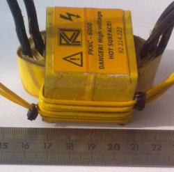
High frequency operation of the transformer is essential to keep the passive energy conversion elements in small size. For this application a custom-made special transformer is developed, the prototype is shown on fig2. with the auxiliary windings. The isolation transformer has composed by a state-of -the -art high frequency ferrite material which exhibits very low power losses in its operation frequency range from 115KHz up to 285KHz. The high current windings of the transformer are made from custom made thin copper layer with high temperature 'class F' insulation laminated rectangular strips.
The Half-bridge serial-resonant ZVS topology is among one of known highest efficiency converters up to date. The converter works above its characteristics resonant frequency in the entire operational range. This type of converter has all of the advantages of soft switching behavior like the switching devices turns on at nearly zero voltage on it and the turn-off losses are also greatly reduced by the capacitive snubbers attached to the power devices. The capacitive snubbering (Cs1,2) used on the switching devices has a strong influence on dV/dt values at commutation transitions and reduces high-frequency ringings. Lower dV/dt and less ringing means lower EMI floor of the converter and less voltage stresses to the output rectification diodes (Do1,2). Compared to the widely-used ZCS serial-resonant converters the ZVS method has much less snubbing requirements and lower thermal losses at the output rectifiers.
Lowered switching losses enable to run the converter at high
frequency without affecting the conversion efficiency. The power
supply is controlled by an embedded microprocessor which
represents several digital signal processing functions also. All
of the enviromental conditions like temperature and input line
voltage are continuously monitored by the processor and driver
signals generated for power switching devices. To maintain the ZVS
operation (fig3.) of the power switching devices a novel PFM/PWM
modulation technique is developed. The actual operation frequency
and PWM values are both changes depends on the output load
conditions. Clear ZVS transitions can be observed on the switching
devices, they are always turns on at nearly zero voltage and the
dV/dt of turn-off transitions are decreased by the parallel
capacitive snubbing elements.
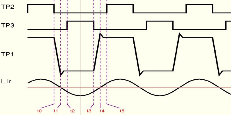
fig1.
High frequency operation of the transformer is essential to keep the passive energy conversion elements in small size. For this application a custom-made special transformer is developed, the prototype is shown on fig2. with the auxiliary windings. The isolation transformer has composed by a state-of -the -art high frequency ferrite material which exhibits very low power losses in its operation frequency range from 115KHz up to 285KHz. The high current windings of the transformer are made from custom made thin copper layer with high temperature 'class F' insulation laminated rectangular strips.
The Half-bridge serial-resonant ZVS topology is among one of known highest efficiency converters up to date. The converter works above its characteristics resonant frequency in the entire operational range. This type of converter has all of the advantages of soft switching behavior like the switching devices turns on at nearly zero voltage on it and the turn-off losses are also greatly reduced by the capacitive snubbers attached to the power devices. The capacitive snubbering (Cs1,2) used on the switching devices has a strong influence on dV/dt values at commutation transitions and reduces high-frequency ringings. Lower dV/dt and less ringing means lower EMI floor of the converter and less voltage stresses to the output rectification diodes (Do1,2). Compared to the widely-used ZCS serial-resonant converters the ZVS method has much less snubbing requirements and lower thermal losses at the output rectifiers.
fig2.
fig3.
The start-up sequence for
reducing the current stresses on the switching devices and
output devices caused by the empty output capacitor block is
preprogrammed into the controller as well as safety shut-down
functions in case of fault or overload.
Moreover we have established a full duplex optically isolated digital communication link (OP1,2) between the processor of power supply and the main system controller in the amplifier. The system controller sees the signals of the amplifier stages and makes a kind of 'feed-forward' regulation of the power supply unit. This way the amplifier is able to change the parameters of power supply before the signs of change would appear on its output voltage.
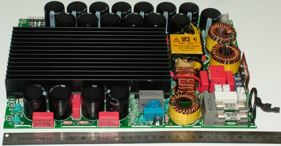
The proposed power supply unit is constructed on a heavy-copper multilayer board with simplified wiring needs. The unit shown on fig 4. fits in a single rack unit height box and requires forced air cooling while is able to deliver 7600 Watts peak power used in the XD/XE amplifier series from PKN Controls.
Moreover we have established a full duplex optically isolated digital communication link (OP1,2) between the processor of power supply and the main system controller in the amplifier. The system controller sees the signals of the amplifier stages and makes a kind of 'feed-forward' regulation of the power supply unit. This way the amplifier is able to change the parameters of power supply before the signs of change would appear on its output voltage.
The proposed power supply unit is constructed on a heavy-copper multilayer board with simplified wiring needs. The unit shown on fig 4. fits in a single rack unit height box and requires forced air cooling while is able to deliver 7600 Watts peak power used in the XD/XE amplifier series from PKN Controls.
fig4.